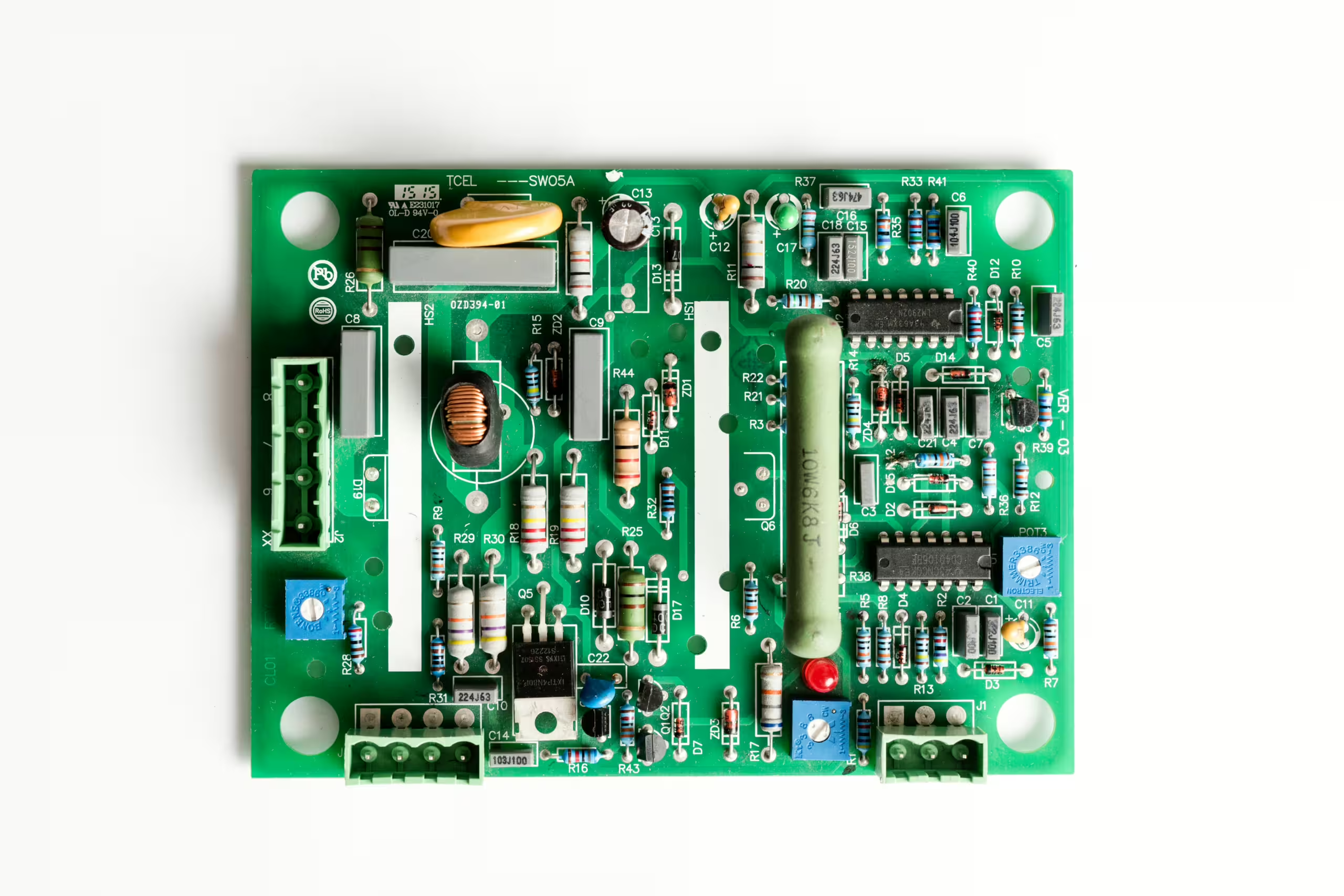
- Explanation of PCB Layer Terms: Topoverlay — This is where the top layer device names are indicated, also known as the top silkscreen or top component legend, such as R1, C5, IC10. Bottomoverlay — Corresponds similarly to the top overlay but for the bottom layer. Multilayer — If you design a 4-layer board and place a free pad or via defining it as multilayer, the pad will automatically appear on all four layers. If it’s defined only for the top layer, then the pad will appear only on the top layer.
- Key Aspects to Consider in 2G+ High Frequency PCB Design: 2G+ high frequency PCBs fall under RF circuit design, not high-speed digital circuit design. Layout (layout) and wiring (routing) should be considered together with the schematic, as layout and wiring can cause distributed effects. Some passive components in RF circuits are defined parametrically and realized with special shaped copper foils, thus requiring EDA tools that support parametric components and can edit special shaped copper foils. Mentor Graphics’ Boardstation has a specialized RF design module that meets these requirements. Also, RF designs generally require specialized RF circuit analysis tools; the most renowned in the industry is Agilent’s EEsof, which interfaces well with Mentor’s tools.
- Rules for Designing Microstrip in 2G+ High Frequency PCB Design: RF microstrip line design requires the use of three-dimensional field analysis tools to extract transmission line parameters. All rules should be stipulated within this field extraction tool.
- Protective Circuits for a Fully Digital Signal PCB with an 80MHz Clock Source: Ensuring the driving capability of a clock should not rely on protective means but rather on using clock driver chips. Concerns about clock driving capability usually stem from multiple clock loads. Using clock driver chips can distribute a single clock signal into multiple ones through point-to-point connections. In choosing a driver chip, besides ensuring basic load matching and signal edge requirements (typically, clocks are edge-triggered), consider the clock delay within the driver chip when calculating system timing.
- Interface Choices for a Standalone Clock Signal Board to Minimize Impact on Clock Signal Transmission: The shorter the clock signal path, the smaller the transmission line effects. Using a separate clock signal board increases signal routing length and also presents grounding and power supply issues. For long-distance transmission, differential signaling is recommended. LVDS signaling can meet driving capacity requirements, although your clock speed is not very high, so it might not be necessary.
- Methods to Reduce Interference from High Frequency Harmonics in Clock Lines: If third harmonics are significant while second harmonics are minimal, it might be due to a 50% duty cycle of the signal, as such a duty cycle does not produce even harmonics. Adjusting the signal’s duty cycle might be necessary. Additionally, for unidirectional clock signals, source-end serial matching is commonly used to suppress secondary reflections without affecting the clock edge rate. The source-end matching value can be calculated using the following formula:
- What is Routing Topology? Topology, also known as routing order, refers to the sequence of connections for networks with multiple ports.
- How to Adjust Routing Topology to Enhance Signal Integrity? The influence of topology on signal quality varies with the direction of network signals, as single-directional, bidirectional, and different signal levels all have different impacts. It is challenging to specify which topology benefits signal quality due to the complexity of the signal directions in the network. Additionally, what topology to use during pre-simulation requires high engineer expertise, understanding circuit principles, signal types, and even routing difficulty.
- How to Arrange Layer Stacking to Reduce EMI Issues? EMI should be considered systemically, as it cannot be resolved by PCB design alone. Layer stacking mainly provides the shortest return path for signals, minimizes coupling areas, and suppresses differential mode interference. Additionally, tightly coupling ground and power layers, with appropriate extensions beyond the power layer, helps suppress common mode interference.
- Why Add Copper Filling? Copper filling serves several purposes: EMC: For large areas of ground or power, copper filling acts as shielding. In special cases, like PGND, it provides protection. PCB Processing Requirements: Often, copper filling is used to ensure effective plating or to prevent warping of the PCB during lamination, especially in layers with sparse routing. Signal Integrity: Provides a complete return path for high-frequency digital signals and reduces DC network routing. Also, it serves for heat dissipation and meets specific device mounting requirements.
- Considerations for Routing in a System Containing DSP and PLD: Considerations depend on the ratio of signal rate to routing length. If the delay of the signal on the transmission line is comparable to the time it takes for the signal to change, signal integrity issues must be considered. Additionally, for multiple DSPs, the topology of clock and data signal routing can affect signal quality and timing, requiring attention.


