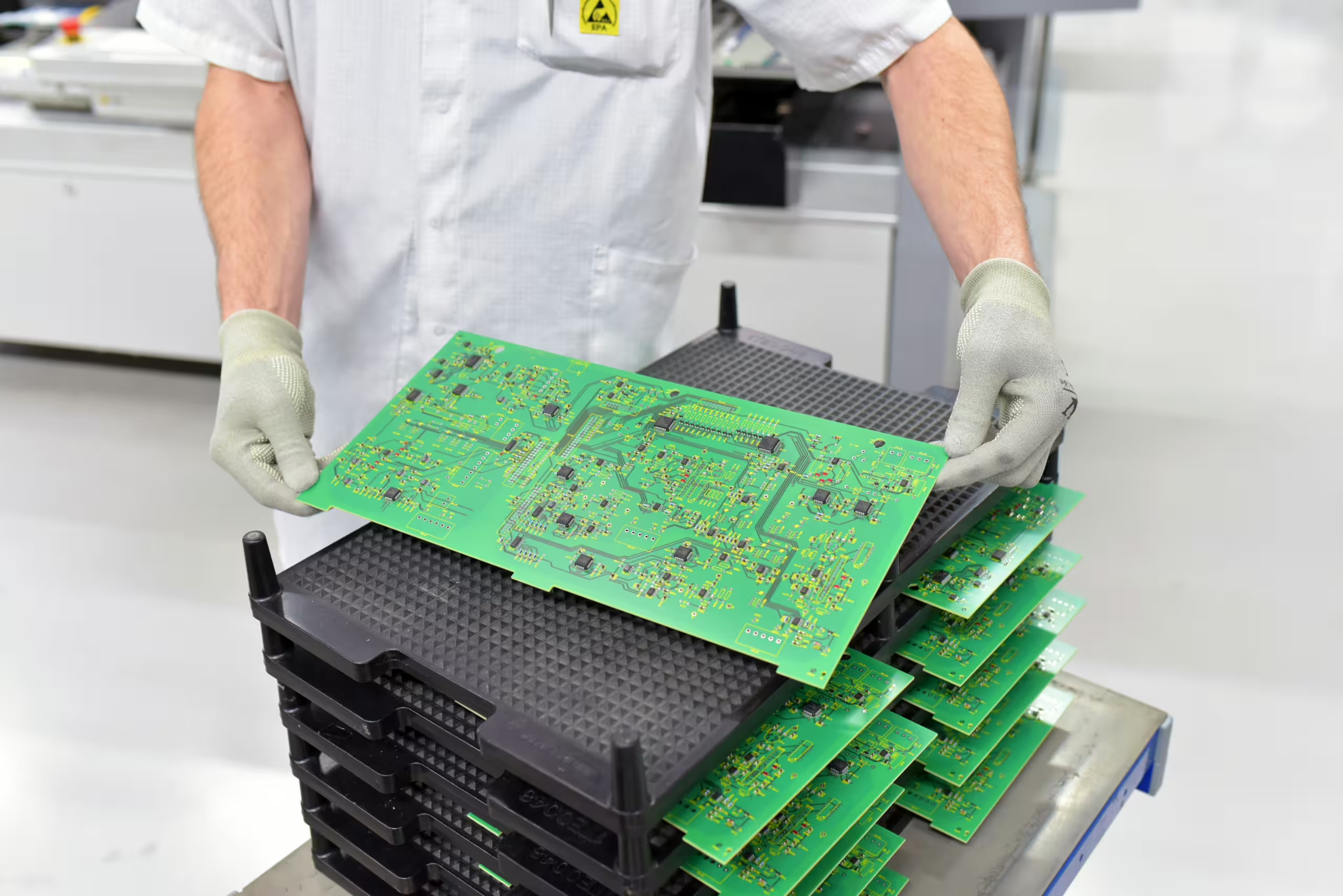
Power Supply Efficiency Testing: Methods, Measurements, and Best Practices
Explore power supply efficiency testing with our detailed guide. Learn key concepts, testing methods, and precautions to enhance power supply performance.
Explore power supply efficiency testing with our detailed guide. Learn key concepts, testing methods, and precautions to enhance power supply performance.
Discover the essentials of RC low-pass filters, focusing on cutoff frequency calculation, impedance optimization, and key design constraints.
Optimize your PCB design with effective Electromagnetic Compatibility (EMC) strategies to tackle common challenges like parasitic impedance and ground connections.
Explore the intricacies of RF PCB design, mastering layout strategies, isolation techniques, and optimal wiring to ensure robust radio communication performance.
How to Manage Layout and Routing to Ensure Stability for Signals Above 50M: In high-speed digital signal routing, the key is to minimize the impact of the transmission line on signal quality. Therefore, layouts for high-speed signals of 100M and above require that signal traces be as short as possible. In digital circuits, high-speed signals…
What is the “Signal Return Path”? The signal return path, also known as return current, is crucial in high-speed digital signal transmission. The current flows from the driver along the PCB transmission lines to the load, and returns to the driver side via the shortest path through the ground or power layer. Dr. Johnson explains…
Explanation of PCB Layer Terms: Topoverlay — This is where the top layer device names are indicated, also known as the top silkscreen or top component legend, such as R1, C5, IC10. Bottomoverlay — Corresponds similarly to the top overlay but for the bottom layer. Multilayer — If you design a 4-layer board and place…
Characteristic Impedance Formulas Commonly Referenced: Microstrip: The formula Z = {87 / [sqrt(Er + 1.41)]} * ln[5.98H / (0.8W + T)] applies where W is the trace width, T is the trace copper thickness, H is the distance from the trace to the reference plane, and Er is the PCB material’s dielectric constant. This formula…
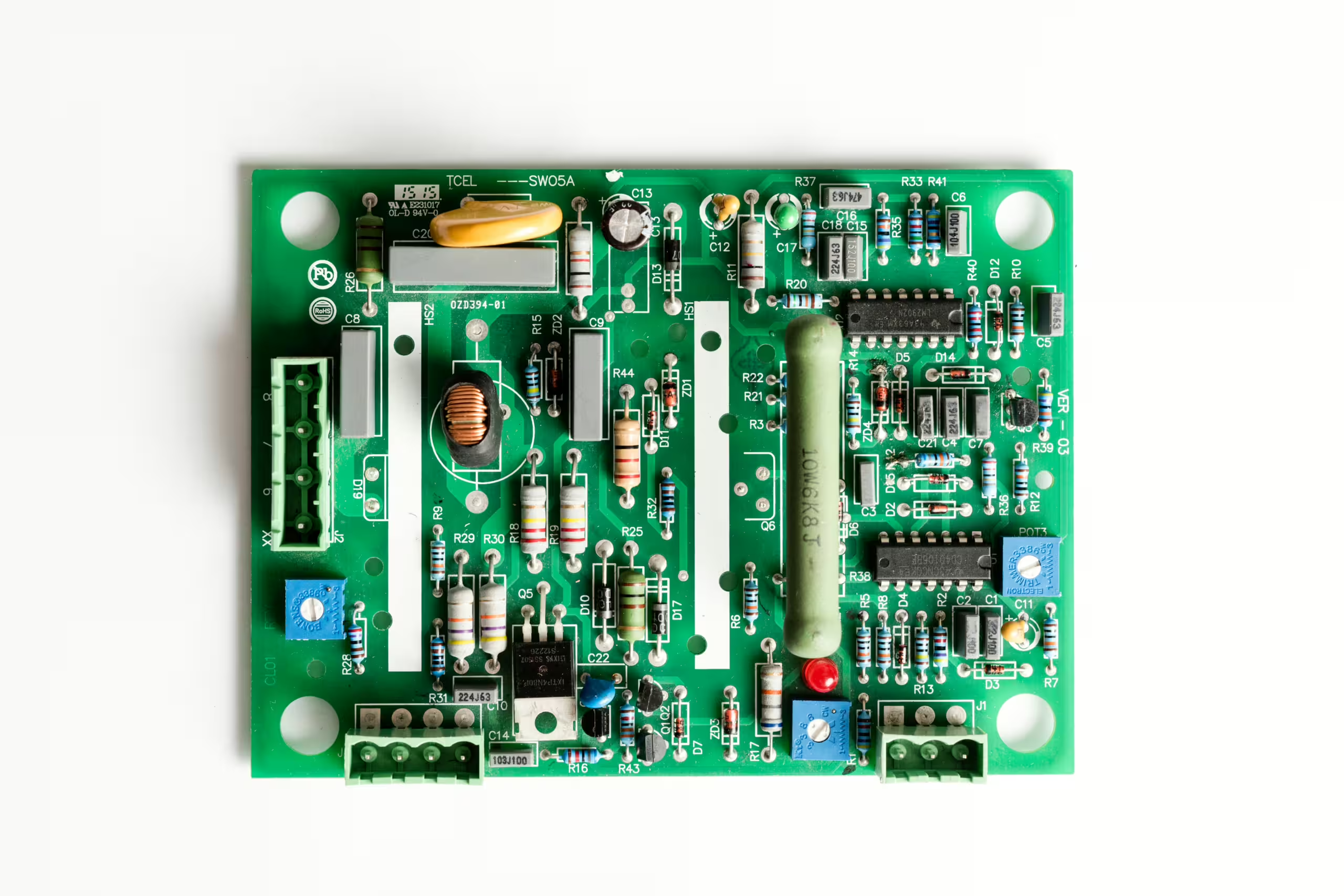
Choosing PCB Materials: To select the right PCB material, one must balance design requirements, manufacturability, and cost considerations. These requirements include both electrical properties and mechanical stability. Material choice is critical when designing very high-speed PCBs (frequencies exceeding GHz). For instance, the popular FR-4 material may not be suitable at several GHz frequencies due to…
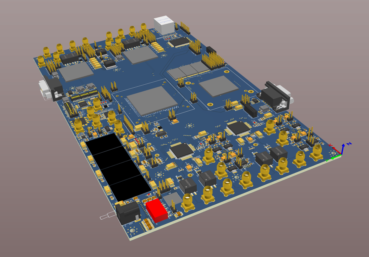
Rockbrain® Corporation’s FPGA-based high-speed signal processing system harnesses the power of Xilinx V7 to deliver superior performance and adaptability.


