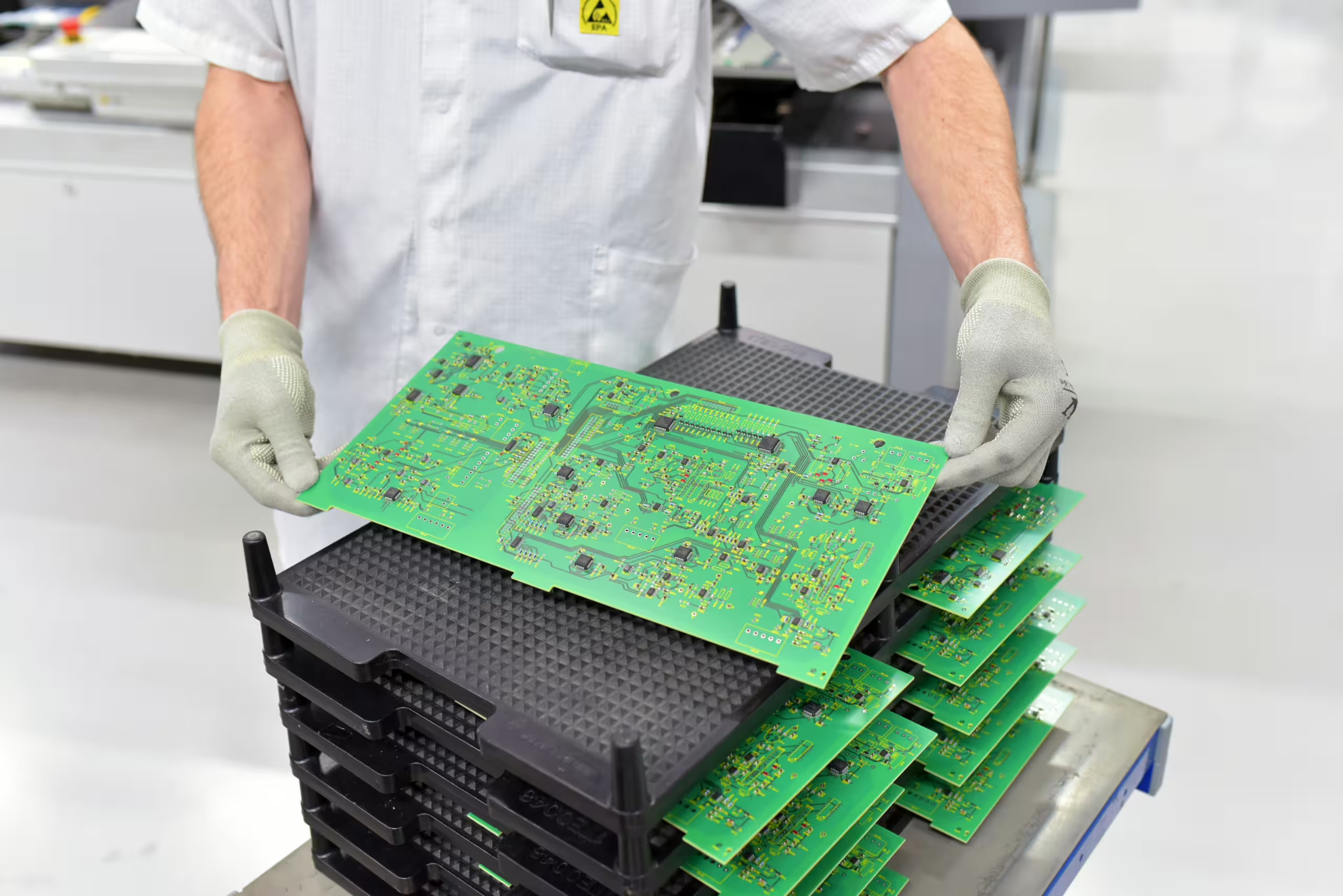
Choosing PCB Materials: To select the right PCB material, one must balance design requirements, manufacturability, and cost considerations. These requirements include both electrical properties and mechanical stability. Material choice is critical when designing very high-speed PCBs (frequencies exceeding GHz). For instance, the popular FR-4 material may not be suitable at several GHz frequencies due to its significant dielectric loss, which heavily impacts signal attenuation. It’s crucial to ensure the dielectric constant and dielectric loss of the material are appropriate for the target frequency range.
Avoiding High-Frequency Interference: To mitigate high-frequency interference, the fundamental strategy involves reducing the electromagnetic interference of high-frequency signals, commonly known as crosstalk. This can be achieved by increasing the separation between high-speed and analog signals or by adding ground guard/shunt traces next to analog signals. Attention should also be paid to the noise interference between digital and analog grounds.
Addressing Signal Integrity in High-Speed Designs: Signal integrity primarily involves impedance matching. Factors influencing impedance matching include the architecture and output impedance of the signal source, the characteristic impedance of the traces, load characteristics, and the topology of the trace layout. Solutions include proper termination and adjusting the trace topology.
Implementing Differential Pair Routing: When routing differential pairs, two key aspects are critical: maintaining equal length of the traces and constant separation (determined by differential impedance), ensuring they remain parallel. This can be accomplished either by routing side-by-side on the same layer or on adjacent layers (over-under), with the former being more common.
Differential Pair Routing for Single-ended Clock Signals: Differential routing only makes sense if both the signal source and the receiver are differential. Therefore, differential routing isn’t applicable for clock signals with a single output.
Adding Matching Resistors to Receiver Differential Pairs: It is common to add matching resistors between receiver differential pairs, typically equal to the differential impedance, to enhance signal quality.
Why Differential Pairs Should Be Close and Parallel: Differential pairs should be routed close together and parallel to maintain consistent differential impedance, which is a crucial parameter in designing differential pairs. Inconsistent spacing can affect signal integrity and timing delays.
Resolving Theoretical Conflicts in Actual Wiring: Generally, isolating digital and analog grounds is correct. Care must be taken to prevent signal traces from crossing split ground regions and to avoid large returning current paths for power and signal lines. Oscillators, being analog positive feedback circuits, require close proximity to chips to ensure stable oscillations and are sensitive to interference, even with ground guard traces.
Resolving Manual vs. Automatic Routing Contradictions for High-Speed Signals: Modern advanced routing software often includes constraint settings to control routing styles and via counts. However, the capabilities and constraints offered by different EDA companies’ routing engines can vary significantly. Factors such as the control over serpentine routing and differential pair separation can influence whether automated routing meets the designer’s intent. Manual routing adjustments also depend heavily on the engine’s capabilities, like trace pushing, via shoving, and their influence on copper pour.
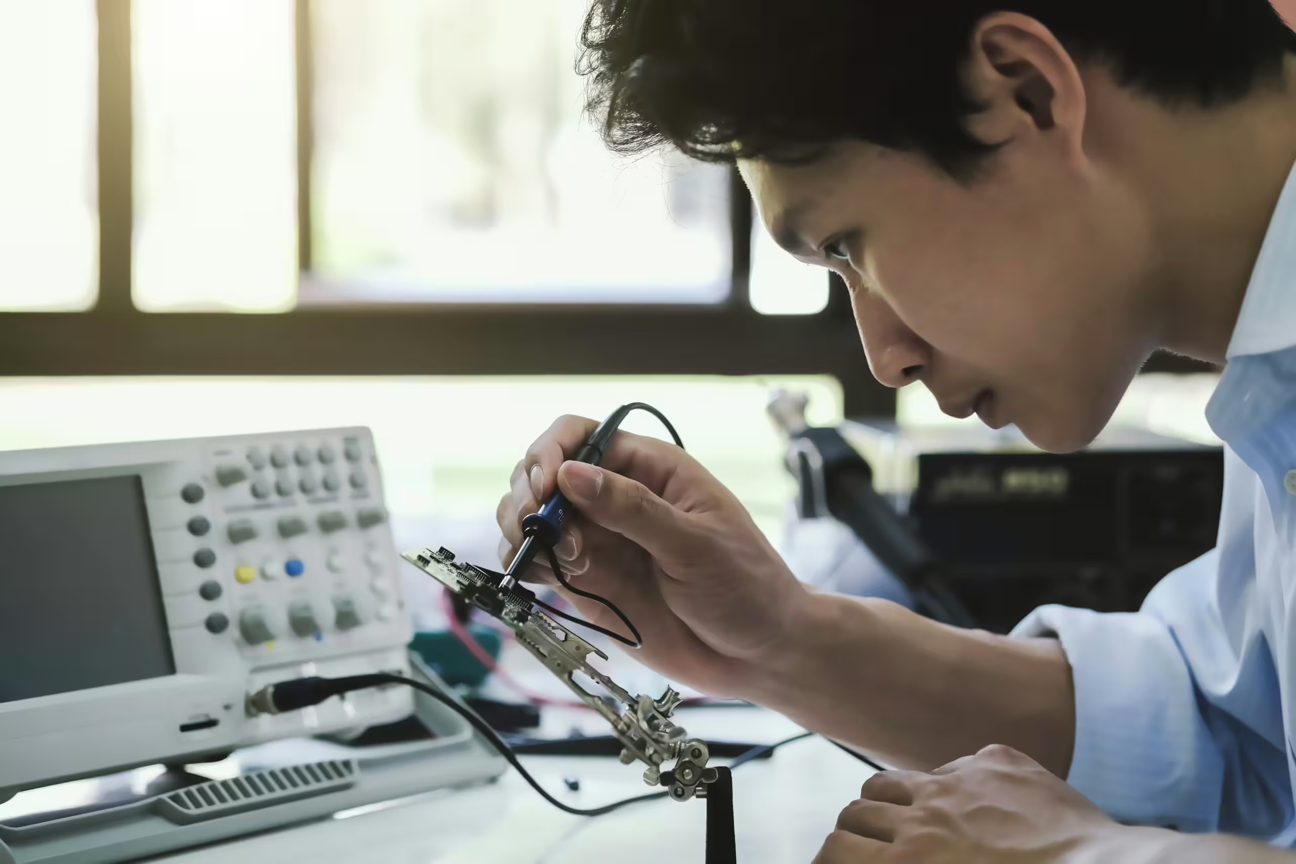
About Test Coupons: Test coupons are used with a Time Domain Reflectometer (TDR) to measure whether the characteristic impedance of a manufactured PCB meets design specifications. Important aspects to control include single-ended and differential pair impedances. Thus, the trace width and spacing on test coupons (for differential pairs) should match the controlled traces. Critical is the positioning of the ground point during measurement to minimize the inductance of the ground lead. The TDR probe’s grounding is usually very close to the measurement signal point, making the placement and method of grounding on the test coupon crucial for compatibility with the probe used.
Copper Filling in Signal Layer Vacancies of High-Speed PCBs: In high-speed PCB design, copper is generally used to fill blank areas, primarily for grounding purposes. However, when copper is placed next to high-speed signal lines, it’s essential to consider the proximity of the copper to these lines as it slightly reduces the characteristic impedance of the traces. Care must also be taken not to affect the characteristic impedance of other layers, such as in a dual stripline configuration.
Calculating Characteristic Impedance Using the Microstrip Model for Signal Lines on Power Planes: Yes, when calculating characteristic impedance, both power and ground planes must be considered as reference planes. For example, in a four-layer board configuration like Top layer-Power layer-Ground layer-Bottom layer, the characteristic impedance model for the top layer traces would use the power plane as the reference plane in a microstrip model.
Automated Test Point Generation in High-Density PCBs for Mass Production: Whether software-generated test points meet production testing requirements depends on whether the test point additions conform to the specifications of the testing equipment. If the traces are densely packed and the specifications for adding test points are strict, it might not be possible to automatically add test points to every trace segment, necessitating manual completion of required test points.
Impact of Test Points on High-Speed Signal Quality: The impact on signal quality depends on how the test points are added and the speed of the signal. Typically, adding test points (not using existing vias or DIP pins as test points) might involve placing them directly on the trace or branching off a small segment from the trace. The former is akin to adding a small capacitor to the trace, while the latter introduces an additional branch. Both scenarios can affect high-speed signals to some extent, with the degree of impact related to the signal’s frequency, speed, and edge rate. The extent of the impact can be assessed through simulation. In principle, smaller test points (still meeting testing equipment requirements) and shorter branches are preferable.
Connecting Ground Lines Between Multiple PCBs in a System: When multiple PCBs in a system are interconnected for signal or power transmission, an equal amount of current that is sent from one board (e.g., Board A to Board B) must return to the originating board (Board A) through the ground layer, as per Kirchhoff’s current law. This return current seeks the path of least impedance. Therefore, at interfaces where power or signals are interconnected, it is crucial to allocate a sufficient number of pins for the ground to reduce impedance and, consequently, noise on the ground layer. Additionally, analyzing the entire current loop, especially in high-current areas, and adjusting the connection of the ground layer or ground wires can help manage the current flow (e.g., creating a low impedance path at certain points to direct most of the current), thereby minimizing the impact on other sensitive signals.