How to Manage Layout and Routing to Ensure Stability for Signals Above 50M: In high-speed digital signal routing, the key is to minimize the impact of the transmission line on signal quality. Therefore, layouts for high-speed signals of 100M and above require that signal traces be as short as possible. In digital circuits, high-speed signals are defined by the rise time delay. Moreover, different types of signals (such as TTL, GTL, LVTTL) require different methods to ensure signal quality.
Requirements and Interference Prevention for PCBs Containing RF, IF, and Low-Frequency Circuits for Outdoor Units: Mixed-signal design poses significant challenges, and there isn’t a perfect solution. Typically, RF circuits are laid out and routed on a separate board within the system, and they might even be housed within a dedicated shielding enclosure. RF circuits are generally single or double-sided boards with simpler circuits, all designed to minimize the impact on distributed parameters of RF circuits and enhance the consistency of the RF system. Compared to the typical FR4 material, RF circuit boards tend to use substrates with high Q-values. These materials have lower dielectric constants, smaller distributed capacitance, higher impedance, and reduced signal propagation delay. In mixed-signal designs, although RF and digital circuits are placed on the same PCB, they are usually segregated into separate RF and digital circuit areas, each with its own layout and routing. They are shielded from each other using ground vias and shielding boxes.
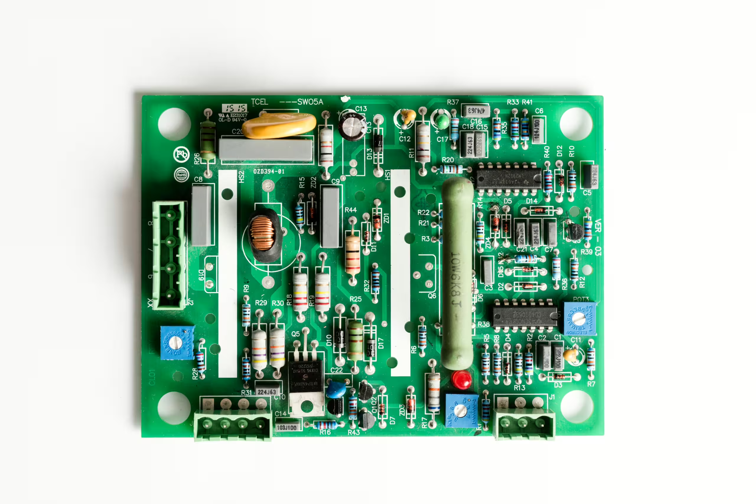
On a 12-layer PCB with three power layers (2.2V, 3.3V, 5V), each occupying a separate layer, how should the ground wiring be handled? Generally, having three power supplies on three separate layers is beneficial for signal quality as it minimizes the likelihood of signal crossing between different planes, which is a critical factor affecting signal quality often overlooked by simulation software. For power and ground layers, they are equivalent for high-frequency signals. In practice, besides considering signal quality, factors like power plane coupling (using adjacent ground planes to reduce the AC impedance of the power plane) and layer stacking symmetry are important considerations.
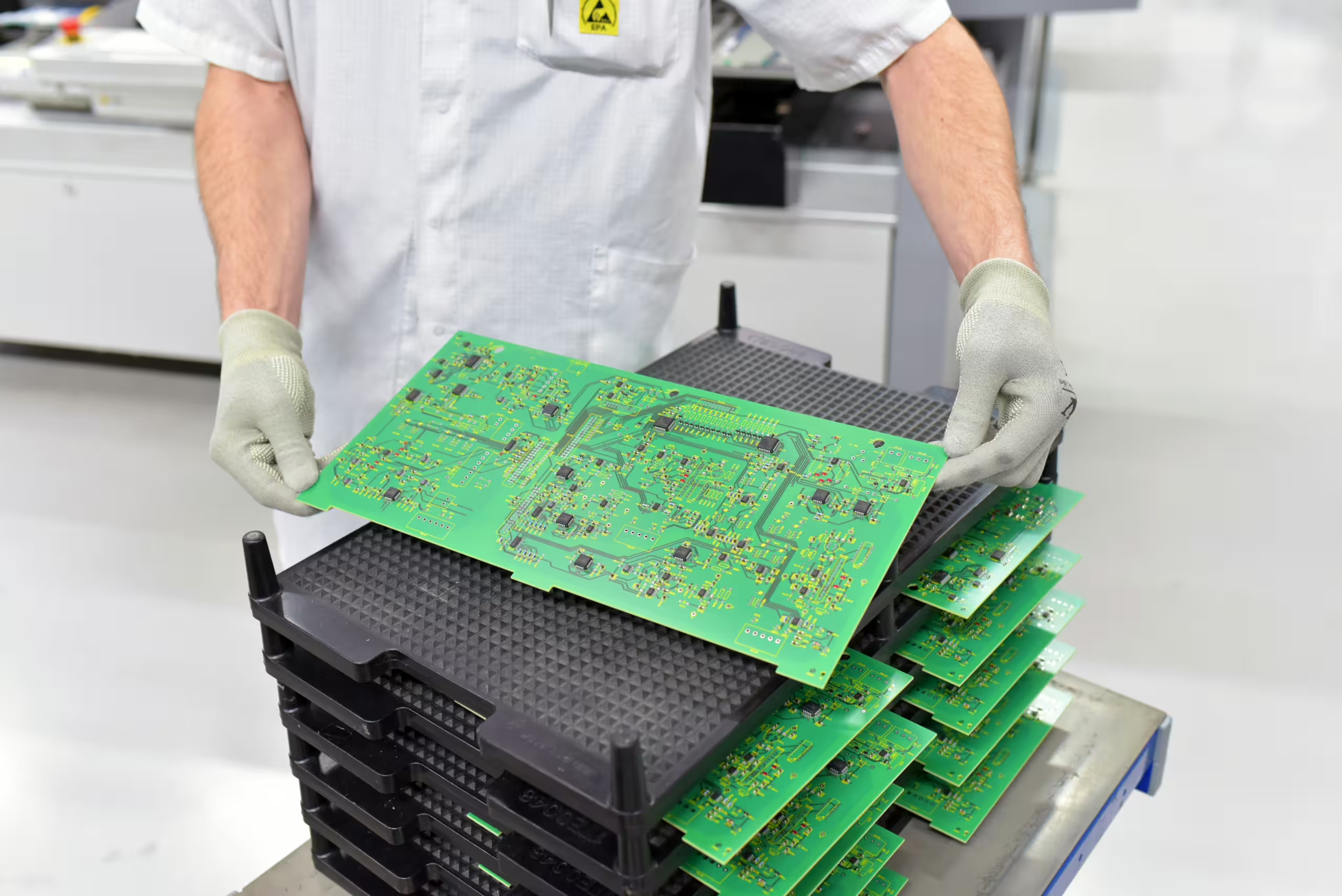
How is a PCB checked for compliance with design specifications before leaving the factory? Many PCB manufacturers perform powered network tests before shipping to ensure all connections are correct. Increasingly, manufacturers are also using X-ray testing to identify faults during etching or lamination processes. For assembled boards, In-Circuit Testing (ICT) is generally used, which requires the addition of ICT test points during PCB design. If issues arise, they can also be diagnosed with specialized X-ray inspection equipment to determine if the issue is due to manufacturing.
Does “mechanical protection” refer to the protection of the chassis? Yes. The chassis should be as sealed as possible, using non-conductive materials where feasible and grounding wherever possible.
When selecting chips, should their inherent ESD characteristics be considered? Regardless of whether it is a double-layer or multi-layer board, it is generally advisable to maximize the area of the ground. When selecting chips, consider the ESD characteristics of the chips themselves, which are usually mentioned in the chip specifications, and even the same type of chip from different manufacturers may perform differently. Paying close attention during design and considering all aspects can help ensure the performance of the finished circuit board. However, ESD issues might still occur, thus making mechanical protection against ESD crucial.
In PCB design, to minimize interference, should the ground traces form a closed loop? In PCB design, it is generally advisable to minimize loop area to reduce interference. Ground traces should not be laid out in a closed loop but rather in a branching pattern, and the area of the ground should be maximized wherever possible.
If a simulator uses one power source and the PCB uses another, should their grounds be connected? It is generally better to use separate power sources to prevent interference between them, but most devices have specific requirements. Since the simulator and PCB use two different power sources, ideally, they should not share a common ground according to this reasoning.
If a circuit consists of several PCBs, should they share a common ground? In a circuit consisting of several PCBs, they are usually required to share a common ground since using multiple power sources within one circuit is impractical. However, if specific conditions allow, using separate power sources can reduce interference.
Designing a handheld product with an LCD and a metal casing that fails to pass the ICE-1000-4-2 ESD test, with CONTACT passing only at 1100V and AIR at 6000V, and ESD coupling tests passing horizontally at 3000V and vertically at 4000V. The CPU’s main frequency is 33MHz. What measures can be taken to pass the ESD test? Handheld products with metal casings are particularly susceptible to ESD issues, and LCDs may also display many defects. If changing the existing metal material is not feasible, it is recommended to add anti-static materials inside the structure, enhance the grounding of the PCB, and find ways to ground the LCD. The specific approach should be tailored to the individual circumstances.